High precision and reliability
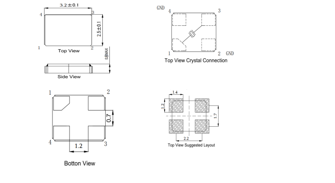
Small package size (3.2×2.5mm)
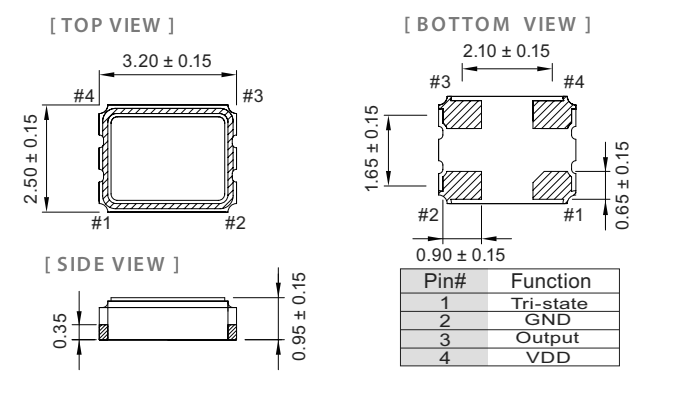
Typical 3.2 x 2.5 x 0.95 mm ceramic SMD package.
Conforms to AEC-Q200
Tight Symmetry (45 to 55%) Available
Operation Voltage: 1.8V, 2.5V, 3.3V
Tri-State Enable/Disable
Typical 3.2 x 2.5 x 0.95 mm ceramic SMD package. low Power Supply Voltage: 3.3V, 2.5V,1.8V. Frequency 32.768kHz. Singled-end Output:CMOS.Temperature Range: -40℃ to 125℃ Operation. Pb-free/RoHS compliant
RTC Module . Smartphone. IoT . Wearable Device – Watch, Medical.
Communication equipment
Multimedia equipment
Industrial equipment
WLAN/WiMAX
Mobile Phone
DSC, Set-Top Box, HDTV
| Size | 3.2*2.5mm |
| Series | BS3225A |
| Supply Voltage | 1.8V,2.5V,3.3V |
| Operating Temperature | 0~70℃,-20~70℃,-30~85℃,-40~70℃,-40~85℃,-50~90℃,-55~95℃,Customized |
| Output Wave | CMOS |
| TriState | With |
| BS3225A Series | |||||||
| Parameters | Value | unit | Conditions | ||||
| MIN | TYP | MAX | |||||
| Center frequency (F0) | 33.333 | MHz | |||||
| Oscillation Mode | fundamental frequency | AT-CUT | |||||
| Frequency deviation (FL) | – | – | ±50 | ppm | +25℃ ± 2℃ | ||
| Temperature frequency difference (TL) | – | – | ±50 | ppm | -55℃~+125℃ | ||
| Supply Voltage(V) | – | 3.3 | – | V | |||
| Excitation power (DL) | – | ±100 | ±300 | uW | |||
| Resonant Resistance (RR) | – | – | 300 | Ω | |||
| Static capacitance (C0) | – | – | 3 | pf | |||
| Insulation Resistance (IR) | 500 | – | MΩ | DC 100V | |||
| Parasitic Attenuation (SPDB) | – | – | -3 | dB | F0±500KHz | ||
| Aging Rate | ±2 | ppm | |||||
| Operating Temperature Range | -55 | – | +125 | ℃ | |||
| Storage Temperature Range | -55 | – | 125 | ℃ | |||
| BS3225A Series | ||||||||||||||
| Parameter | 3.3v | 2.5V | 1.8V | Unit | Condtions | |||||||||
| Min. | Max. | Min. | Max. | Min. | Max. | |||||||||
| Supply Voltage Variation | VDD-5% | VDD+5% | VDD-5% | VDD+5% | VDD-5% | VDD+5% | V | |||||||
| Frenquency Range | 1.25 | 125 | 1.25 | 125 | 1.25 | 125 | MHz | |||||||
| Standard Frequency | 24, 26, 30, 40 | MHz | ||||||||||||
| Transition Time Rise Time / Fall Time | - | 3 | - | 4 | - | 5 | nSec | 1.25MHz Fo < 10MHz | ||||||
| - | 3 | - | 3 | - | 4 | 10MHz Fo < 20MHz | ||||||||
| - | 3 | - | 3 | - | 4 | 20MHz Fo < 80MHz | ||||||||
| - | 3 | - | 3 | - | 4 | 80MHz Fo < 125MHz | ||||||||
| Supply Current | - | 15 | - | 10 | - | 7 | uA | At 15pF Load | ||||||
| - | 1.5 | - | 1.5 | - | 1.2 | No Load Condition, 1.25MHz Fo < 10MHz | ||||||||
| - | 2 | - | 2 | - | 1.5 | No Load Condition, 10MHz Fo < 20MHz | ||||||||
| - | 3 | - | 2.5 | - | 1.5 | No Load Condition, 20MHz Fo < 80MHz | ||||||||
| - | 8 | - | 7 | - | 5 | No Load Condition, 80MHz Fo < 125MHz | ||||||||
| Duty Cycle | 45 | 55 | 45 | 55 | 45 | 55 | % | |||||||
| Output Level | Output High | 2.97 | - | 2.25 | - | 1.62 | - | V | ||||||
| Output Low | - | 0.33 | - | 0.25 | - | 0.18 | V | |||||||
| Tri-State Mode (Input to Pin 1) | Enable | 2.31 | - | 1.75 | - | 1.26 | V | |||||||
| Disable | - | 0.99 | - | 0.75 | - | 0.54 | ||||||||
| Stand by Current | - | 10 | - | 10 | - | 10 | uA | @-40℃ to 85℃ | ||||||
| - | 20 | - | 20 | - | 20 | uA | @-40℃ to 125℃ | |||||||
| Output Loading | 15 | 15 | 15 | pF | ||||||||||
| Period Jitter (Pk-Pk) | - | 40 | - | 40 | - | 40 | pSec | |||||||
| RMS Phase Jitter | - | 1 | - | 1 | - | 1 | pSec | 12kHz to 20MHz | ||||||
| Aging | - | ±3 | - | ±3 | - | ±3 | ppm | @ 25℃, First Year | ||||||
| Storage Temp. Range | -55 | 125 | -55 | 125 | -55 | 125 | ℃ | |||||||
| FREQ. STABILITY vs. TEMP. RANGE | ±20ppm | ±25ppm | ±50ppm | |||||||||||
| -10~+60 | Available | Available | Available | |||||||||||
| -20~+70 | Conditional | Available | Available | |||||||||||
| -40~+85 | Not Available | Available | Available | |||||||||||
| Note: not all combination of options are available. Other specifications may be available upon request. | ||||||||||||||


| Parameter | Condition | |||||||||||||
| Temperature Stress Test | IEC60068, GJB360B | |||||||||||||
| Mechanical Stress Test | IEC60068, GJB360B | |||||||||||||
| EMC Test (ESD) | IEC61000, JESD22 | |||||||||||||
| Solderability | EIA/JESD22-B102-C | |||||||||||||
| Contact Pads | Gold over Nickel | |||||||||||||
| RoHS | RoHS Directive 2011/65/EU Annex II Recasting 2002/95/EC | |||||||||||||
| Test item | Specification | Conditions | |||||
| Drop Test | GB/T2423.8 | 150CM height,fall freely onto concrete floor 3 times. | |||||
| Mechanical Shock | GB/T2423.5 | Device are shocked to half sine wave (1000G) three mutually perpendicular axes each 3 times. 0.5m sec.duration time. | |||||
| Vibration Test | GB/T2423.10 | Amplitude 1.52mm Time 20 min Enable Crystal from 10~2000Hz, X,Y,Z horizontal, 1time/ 2hours | |||||
| Solderability Test | IEC60068-2-58 | Solderabiliity: 245±5℃ Height: 0.5mm Time: 3±0.5second Scaling powder: rosin resin methanol solvent (1:4) | |||||
| High Temp Storage | GB/T2423.2 | 500±12 hours at +125℃±2℃ | |||||
| Low Temp Storage | GB/T2423.1 | 500±12 hours at -40℃±2℃ | |||||
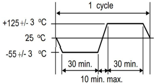
| TEMP CYCLING TEST | GB/T2423.22 | 10 cycles as below table
| |||||
| TEMP &HUM CYCLING TEST | GB/T2423.3 | Temperature:85℃±3℃ Humidity:85% 500h | |||||

Eg: BC3225AI105-32.000-3.3V

Example: BS3225AD3I505CN20
Disclaimer: Xtaltq Technologies Co., Limited reserves the right to make changes to the product(s) and/or information contained herein without notice. No liability is assumed as a result of their use or application. No rights under any patent accompany the sale of any such product(s) or information.
 English
 français
 Deutsch
 Español
 русский


